Equipment & materials
Oxide Wafers
Oxidized silicon substrates for semiconductor and microfabrication processes.
View product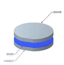
Specify device layer, buried oxide, handle wafer and orientation for your application.
Share your application and target specification for product selection.
These ranges are reference specifications from the 2022 product information. Please request current availability and confirm your required wafer specification.
| Wafer diameters | 100 / 125 / 150 / 200 mm |
|---|---|
| Handle thickness | 200–1000 µm for 100/125/150 mm; 500–750 µm for 200 mm |
| Stack thickness | 280–1250 µm |
| Buried oxide | 0.2–5 µm thermal oxide |
| Device layer | ≥1.5 µm for 100/125/150 mm; 5–300 µm for 200 mm |
| Orientation | <100> / <111> / <110> |
Reference information: 2022 technical ranges; included in the September 2025 portfolio. Final specifications are confirmed in the quotation. Ask a technical question ↗
Oxidized silicon substrates for semiconductor and microfabrication processes.
View productLithium niobate and lithium tantalate substrates for optical and electronic applications.
View productOptical quartz substrates with application-specific dimensions and surface requirements.
View productShare your application, substrate and target specification.