AMIES
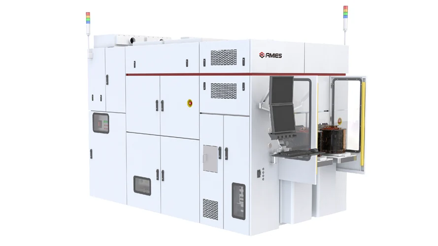
AMIES FEOL Laser Annealing
FEOL Laser Annealing for semiconductor and advanced packaging applications.
View product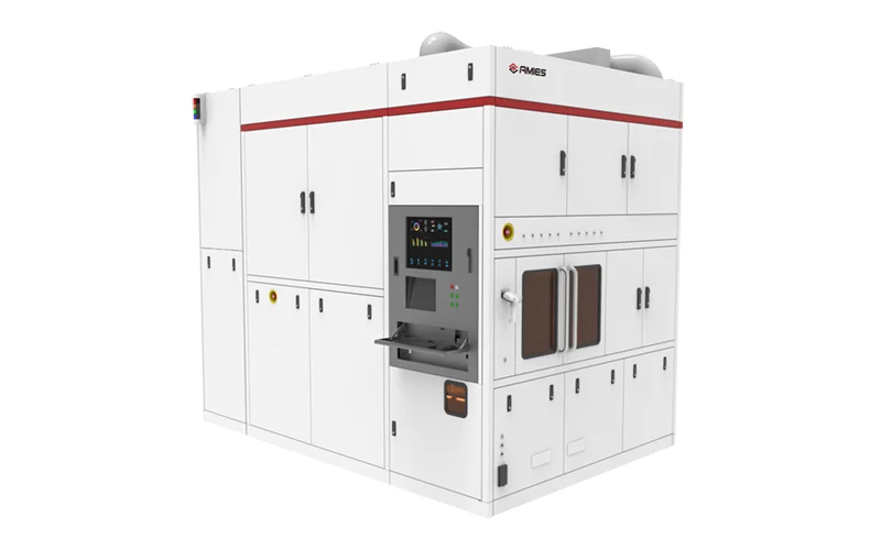
Manufacturer-stated development platform for compound semiconductor lithography. Confirm current product maturity and configuration.
Share your application and target specification for product selection.
Manufacturer-stated development specifications. The brochure scheduled first-prototype acceptance for the second half of 2025; completed acceptance and current product maturity require confirmation. Manufacturer reference information; supply scope and configuration confirmed on enquiry.
| Resolution | 0.35 µm L/S |
|---|---|
| Machine-to-machine overlay | ≤40 nm |
| Substrate sizes | 2 / 3 / 4 / 6 / 8 inches |
Final specifications are confirmed in the quotation. Ask a technical question ↗
FEOL Laser Annealing for semiconductor and advanced packaging applications.
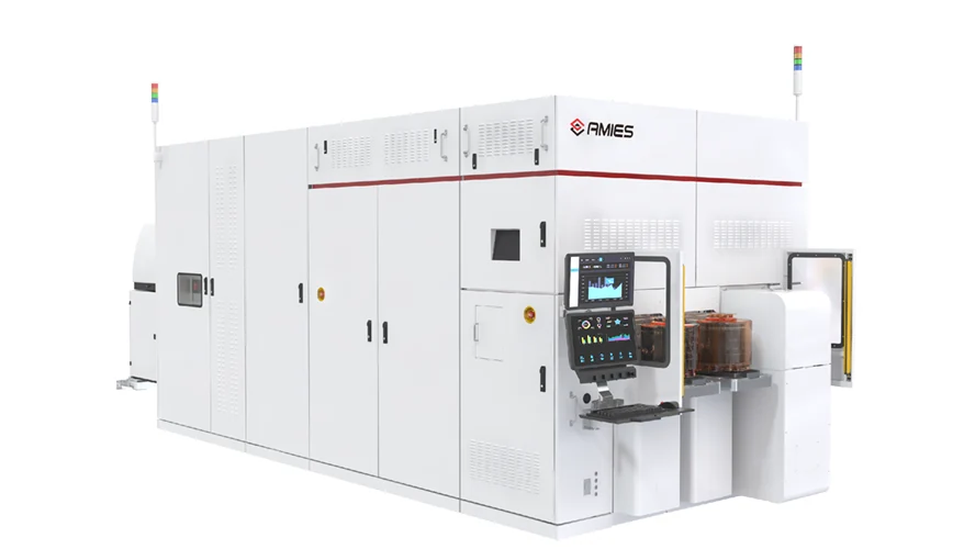
View productPower Device Laser Annealing for semiconductor and advanced packaging applications.
View productOverlay Metrology for semiconductor and advanced packaging applications.
View productShare your application, substrate and target specification.