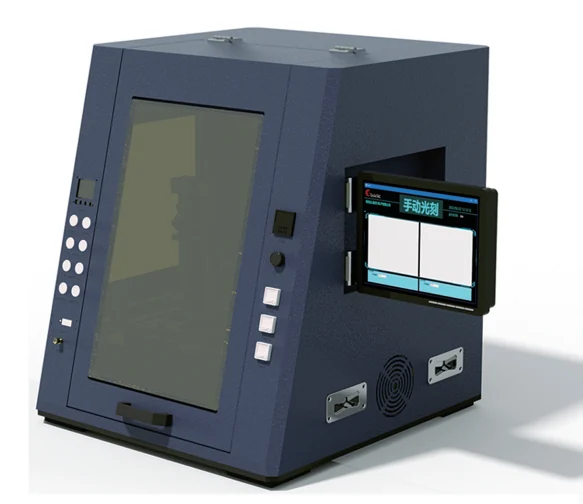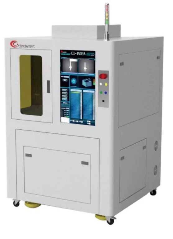
Equipment & materials
WEM2000 Maskless Wafer Writer
Maskless exposure for research, prototyping and small-batch wafer processing.
View product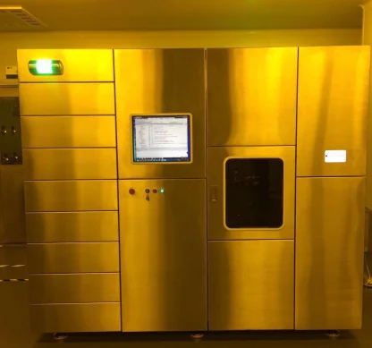
Laser direct writing for photomasks, wafers and microfabrication applications.
Share your application and target specification for product selection.
The reference values below describe the LP3000 exposure modes in the September 2025 product information. Each slash-separated value follows the exposure-mode order. Confirm the required configuration in your quotation.
| Imaging area | Up to 9 × 9 inches. |
|---|---|
| Exposure modes | 1st / 2nd / 3rd |
| Address grid | 10 / 30 / 50 nm |
| Minimum structure | 0.5 / 0.8 / 1.5 µm |
| Write speed | 27 / 50 / 220 mm²/min |
| Fast-mode write speed | 27 / 110 / 440 mm²/min |
| Edge roughness (3σ) | 50 / 70 / 110 nm |
| CD uniformity (3σ) | 50 / 80 / 120 nm |
| Alignment accuracy (3σ) | 70 / 100 / 200 nm |
Reference information: 2025-09. Final specifications are confirmed in the quotation. Ask a technical question ↗
Maskless exposure for research, prototyping and small-batch wafer processing.
View productManual contact lithography with UV LED illumination for small substrates.
View productAutomatic mask alignment and exposure for 150 mm and 200 mm wafers.
View productShare your application, substrate and target specification.