YSD
LP3000 Direct-Write Lithography System
Laser direct writing for photomasks, wafers and microfabrication applications.
View product
Maskless exposure for research, prototyping and small-batch wafer processing.
Share your application and target specification for product selection.
Specifications are reference information; available configurations, performance and lead time are confirmed in your quotation.
| Minimum lines and spaces | 2 µm |
|---|---|
| Minimum feature size | 1 µm |
| CD uniformity (3σ) | 500 nm |
| Edge roughness (3σ) | 150 nm |
| Frontside overlay (3σ) | 500 nm |
| Maximum write speed | 1200 mm²/min |
| Light source (undated equipment sheet) | 405 nm or 375 nm |
| Substrate thickness (undated equipment sheet) | 0.1–5 mm |
| Autofocus dynamic range (undated equipment sheet) | 150 µm |
| Optional functions (undated equipment sheet) | Backside alignment; EFEM |
Reference information: September 2025 company information and an undated equipment sheet, as noted in the table. Final specifications are confirmed in the quotation. Ask a technical question ↗
Laser direct writing for photomasks, wafers and microfabrication applications.
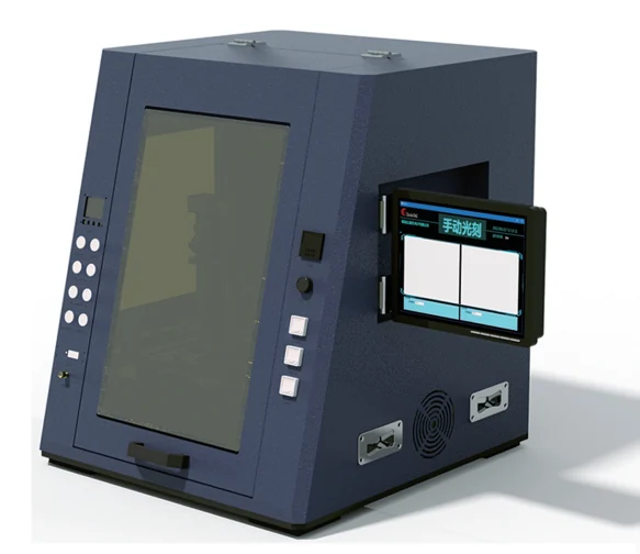
View productManual contact lithography with UV LED illumination for small substrates.
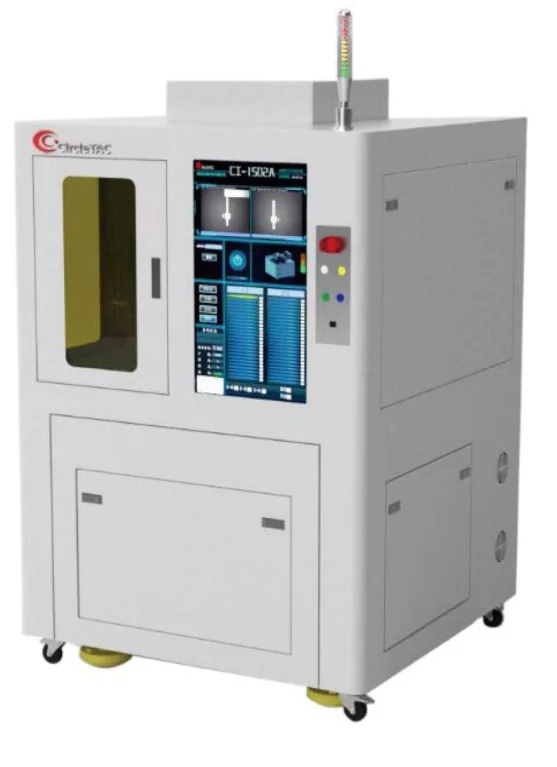
View productAutomatic mask alignment and exposure for 150 mm and 200 mm wafers.
View productShare your application, substrate and target specification.