YSD
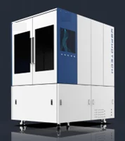
LP3000 Direct-Write Lithography System
Laser direct writing for photomasks, wafers and microfabrication applications.
View product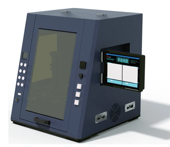
Manual contact lithography with UV LED illumination for small substrates.
Share your application and target specification for product selection.
Specifications are reference information; available configurations, performance and lead time are confirmed in your quotation.
| Exposure type | Single-sided contact exposure |
|---|---|
| Exposure area | 105 × 105 mm |
| Illumination nonuniformity | ≤5% |
| Illumination intensity | 0–25 mW/cm²; higher intensity customizable |
| Wavelength | 405 / 365 nm; 405 nm default |
| Resolution | 2 µm |
| Overlay accuracy | 2 µm |
| Wafer size | ≤Ø102 mm |
| Substrate thickness | ≤5 mm |
| Mask size | ≤127 × 127 mm |
| Dimensions | 750 × 700 × 800 mm |
Reference information: 2025-09. Final specifications are confirmed in the quotation. Ask a technical question ↗
Laser direct writing for photomasks, wafers and microfabrication applications.
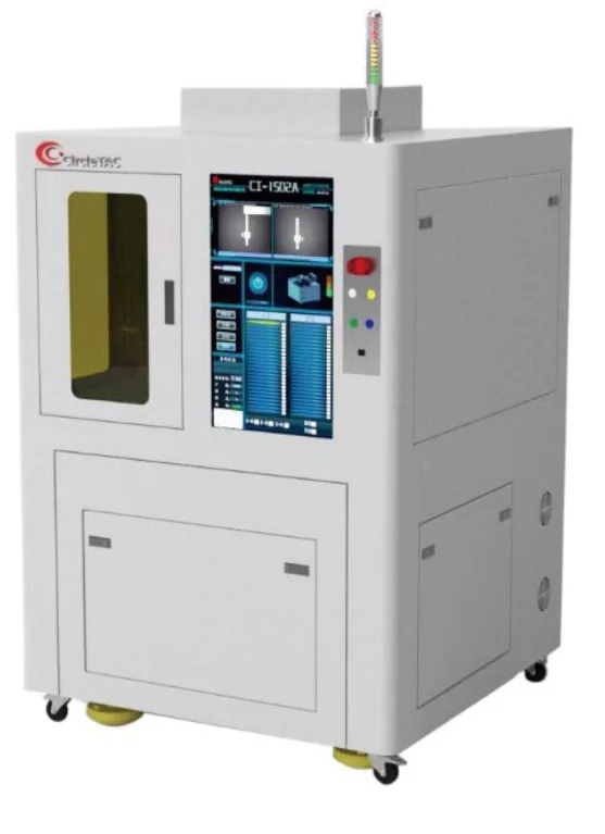
View productMaskless exposure for research, prototyping and small-batch wafer processing.
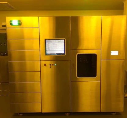
View productAutomatic mask alignment and exposure for 150 mm and 200 mm wafers.
View productShare your application, substrate and target specification.