ZC Optoelectronics
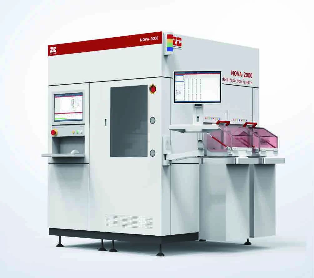
NOVA-2000 SiC Wafer Inspection
Optical defect inspection for polished and epitaxial silicon carbide wafers.
View product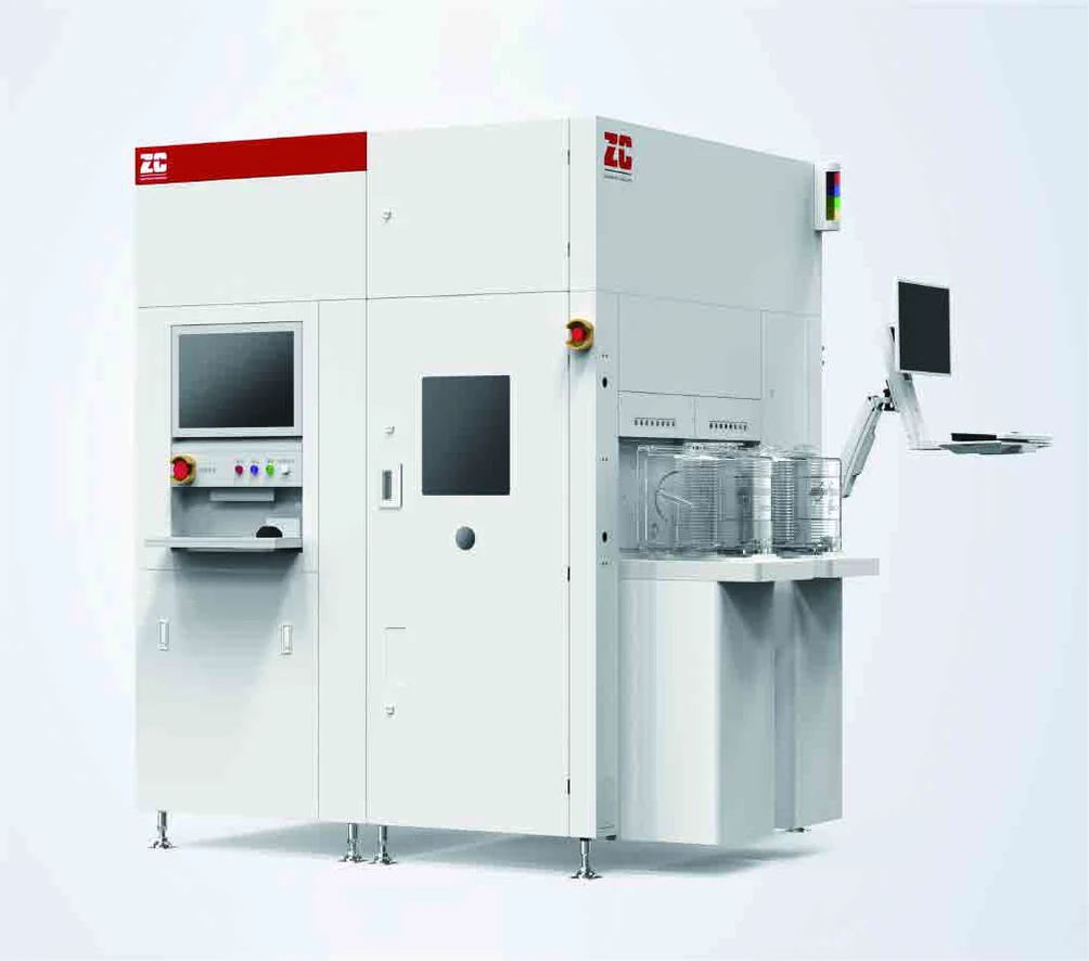
Optical wafer defect inspection. Specify wafer material, diameter and target defect size.
Share your application and target specification for product selection.
Specifications are reference information; available configurations, performance and lead time are confirmed in your quotation. Manufacturer reference information; supply scope and configuration confirmed on enquiry.
| Wafer size | 300 mm |
|---|---|
| Sensitivity | Better than 26 nm |
| Throughput | ≥67 WPH at 300 mm |
Reference information: 2026-03. Final specifications are confirmed in the quotation. Ask a technical question ↗
Optical defect inspection for polished and epitaxial silicon carbide wafers.
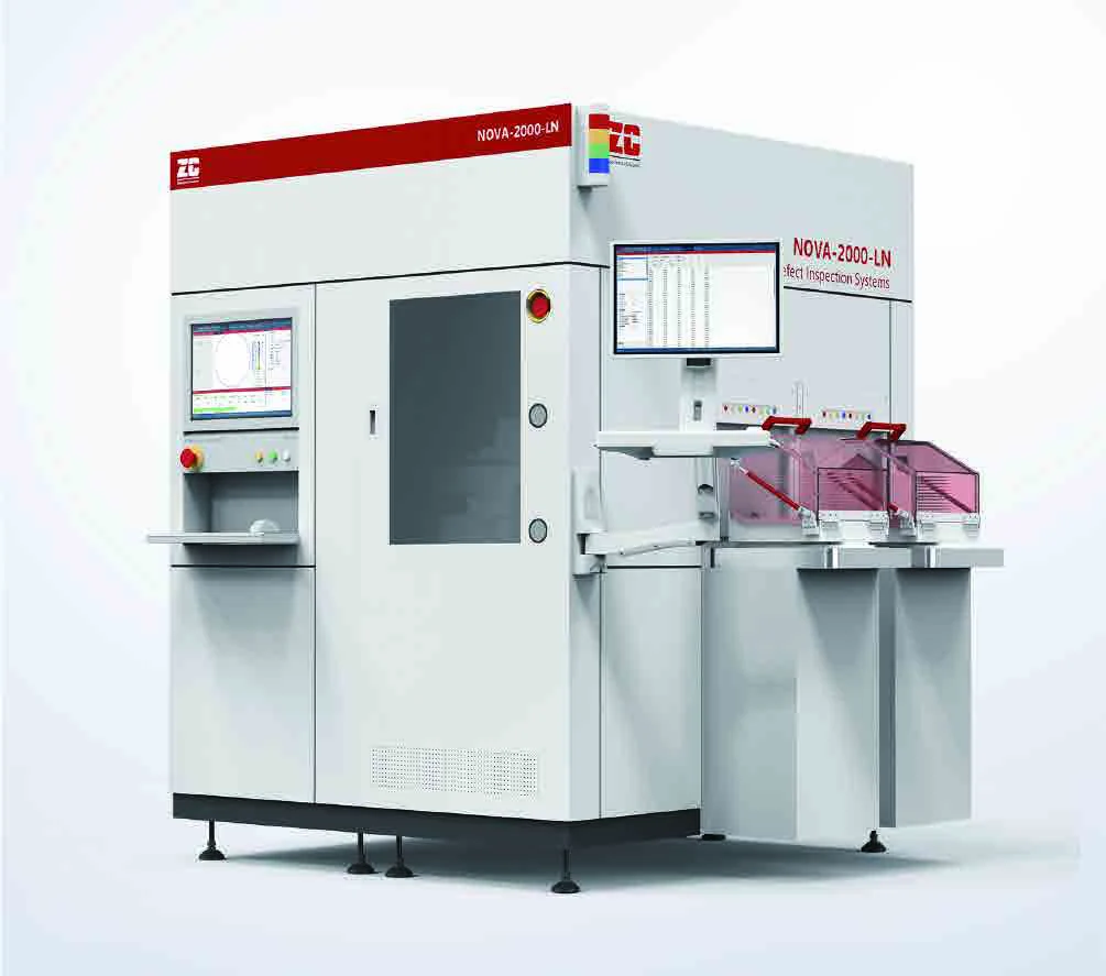
View productDefect inspection for lithium niobate and lithium tantalate substrates.
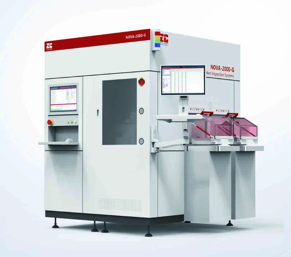
View productOptical defect inspection for glass wafers.
View productShare your application, substrate and target specification.